8.5 KiB
Transmission Lines
Superposition
All solutions to this differential equation have the form
\begin{align}
V(t, z) = e^{j (\omega t - vz)} + e^{j (\omega t + vz)}
\end{align}
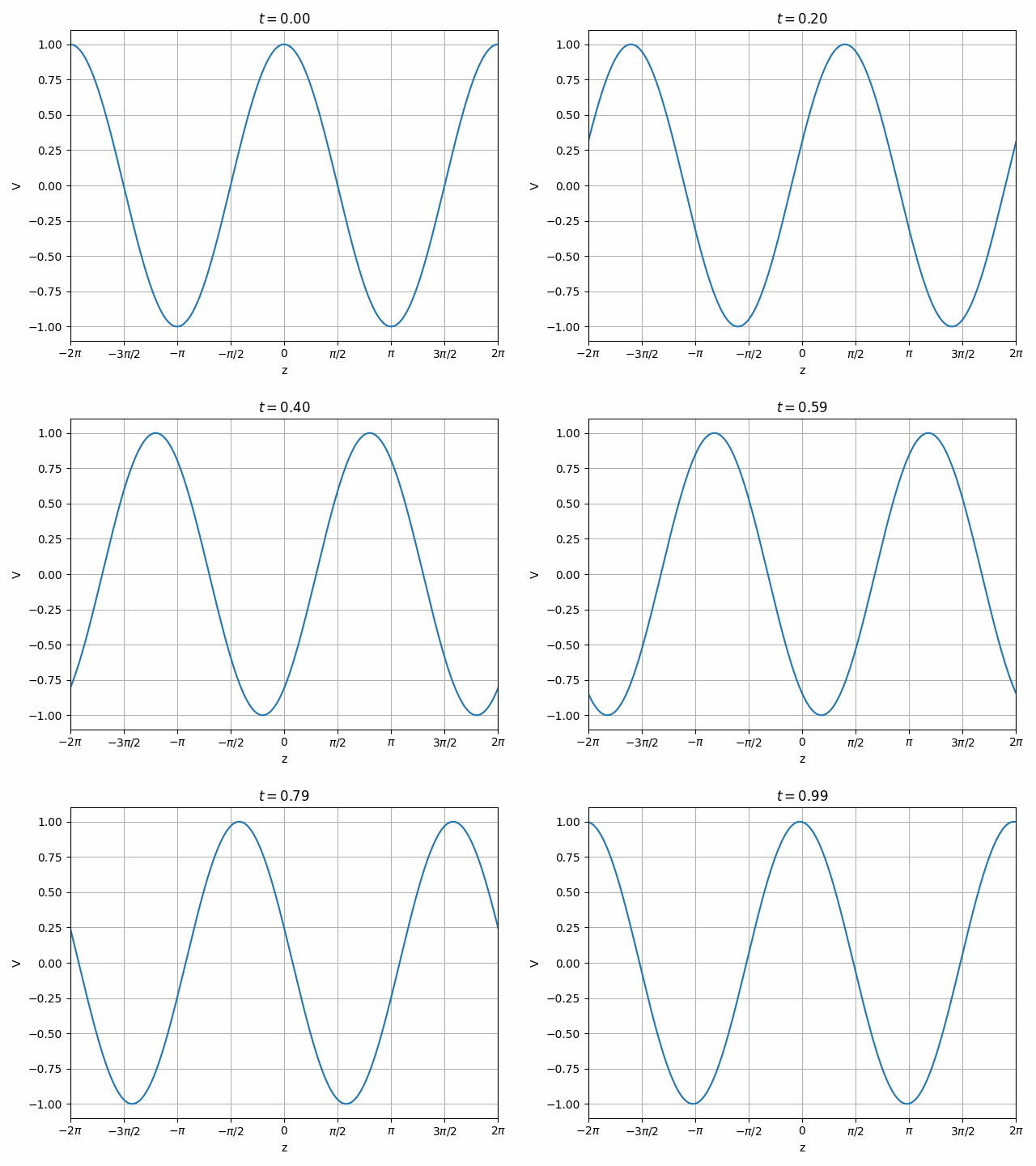
Therefore we can look at a transmission line as having the superposition of two independent waves propagating forward (toward +z) and in reverse (toward -z).
\begin{align}
V_f(t, z) &= e^{j (\omega t - vz)} \\
V_r(t, z) &= e^{j (\omega t + vz)}
\end{align}
Reflections
At the end of a transmission line, voltage and current are related by the impedance of the load Z_L.
Assuming the load is situated at z=0 the following boundary conditions are imposed:
\begin{align}
\hat{I}(z=0) &= \hat{I}_f(z=0) - \hat{I}_r(z=0) \\
\hat{V}(z=0) &= \hat{V}_f(z=0) + \hat{V}_r(z=0) \\
\hat{V}(z=0) &= Z_L\hat{I}(z=0)
\end{align}
We can already relate voltage and current for both forward and reverse propagating waves on the transmission line.
\begin{align}
\hat{V}_f(z) &= Z_0\hat{I}_f(z) \\
\hat{V}_r(z) &= Z_0\hat{I}_r(z)
\end{align}
By combining these constraints we can relate the reverse wave to the forward wave due to the load:
\begin{align}
Z_0\hat{I}_f(z=0) + Z_0\hat{I}_r(z=0) &= Z_L\big(\hat{I}_f(z=0) - \hat{I}_r(z=0)\big) \\
\hat{I}_r(z=0) &= \frac{Z_L - Z_0}{Z_L + Z_0} \hat{I}_f(z=0) \\
\hat{V}_r(z=0) &= \frac{Z_L - Z_0}{Z_L + Z_0} \hat{V}_f(z=0)
\end{align}
We define the reflection coefficient as this ratio:
\begin{align}
\Gamma &= \frac{\hat{V}_r(z=0)}{\hat{V}_f(z=0)} \\
&= \frac{Z_L - Z_0}{Z_L + Z_0}
\end{align}
Note that if Z_L = Z_0 then \Gamma = 0 and there is no reflection. This is generally desired since no power is lost to a reflection and resonances need not be considered (we will look at this in a moment).
| Condition | \Gamma |
|---|---|
| Matched | 0 |
| Open | 1 |
| Short | -1 |
Also note that this is only valid at z=0 since the phase of \hat{V}_f and \hat{V}_r vary with opposite signs as we move along the transmission line so their relationship changes with position.
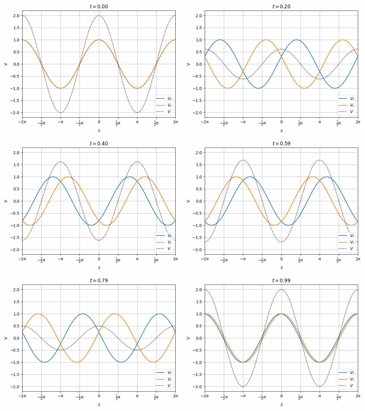
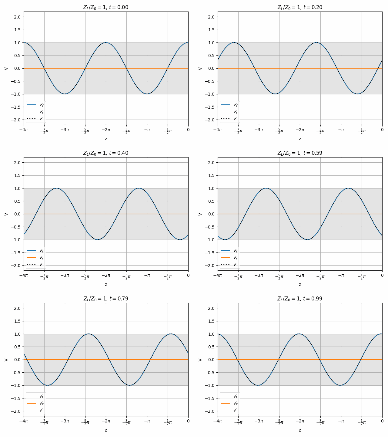
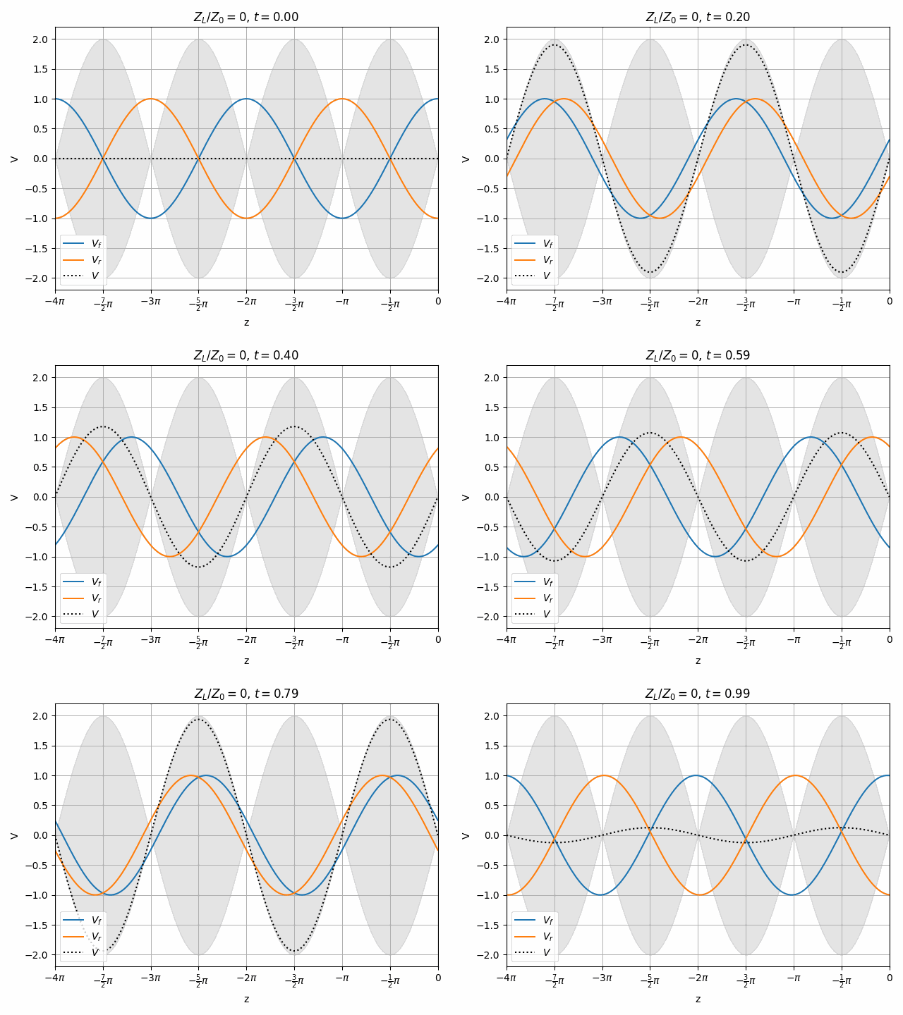
A perfectly matched load results in no reflected wave.
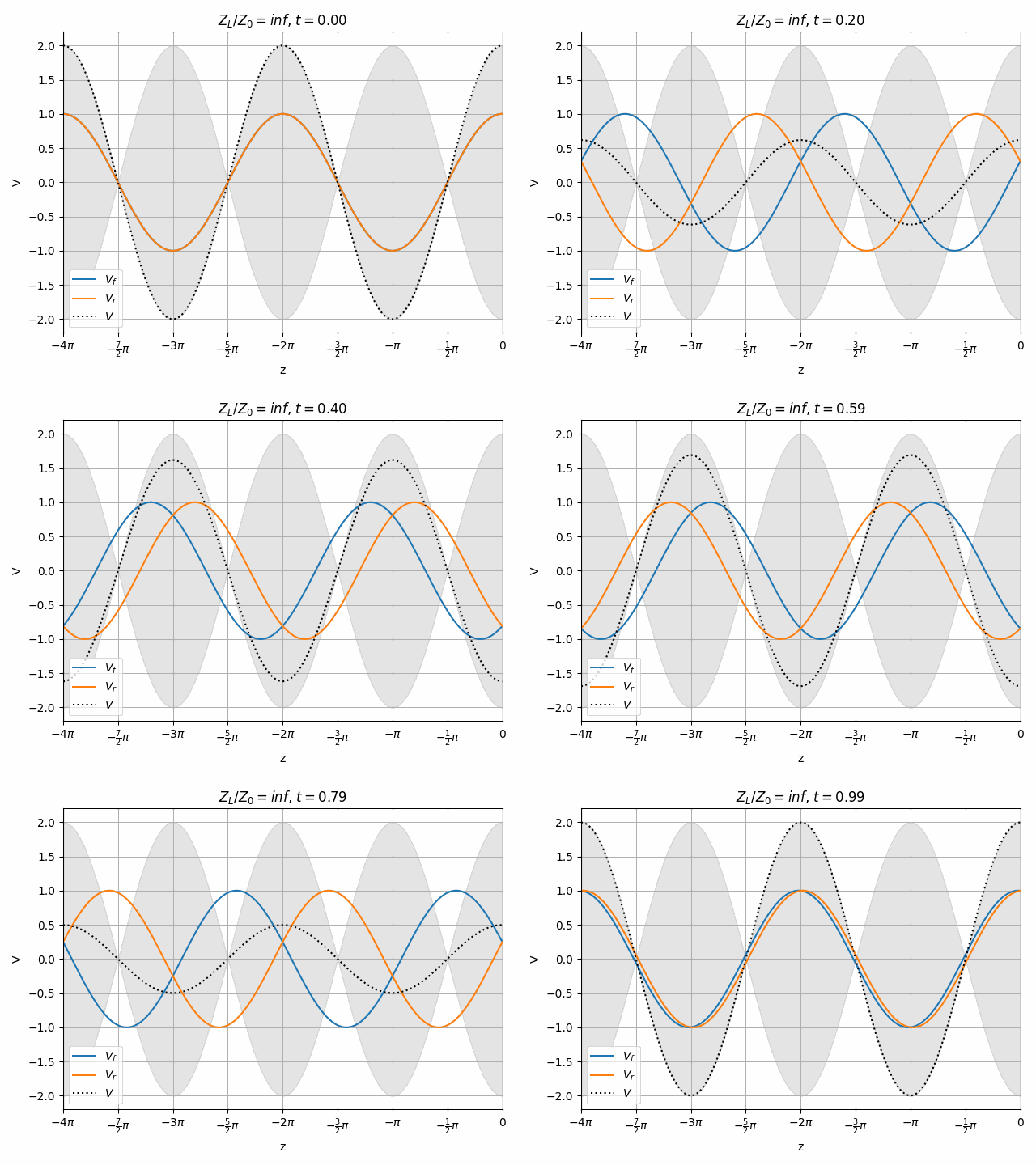
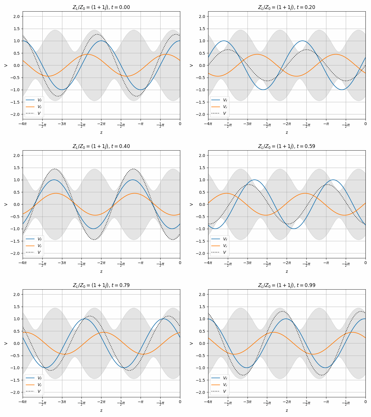
Open and short circuits both have locations where no voltage is seen. Note that both of these cases have an equal amplitude reflected wave, they just have different phase. This is actually true of all lossless loads (ideal capacitor and inductor as well).
It is also worth noting that the peak voltage on the line is 2V when we only excited it with 1V. How is this possible? Remember that there is another end of the transmission line on the left which could cause a re-reflection of V_r to combine with V_f however we are assuming no such reflection exists. This means that the impedance seen at the left end of the transmission line must be matched to Z_0, meaning that the driver has a series impedance equal to Z_0. Therefore V_f = \frac{1}{2} V_{source} and the total voltage V never exceeds V_{source}.
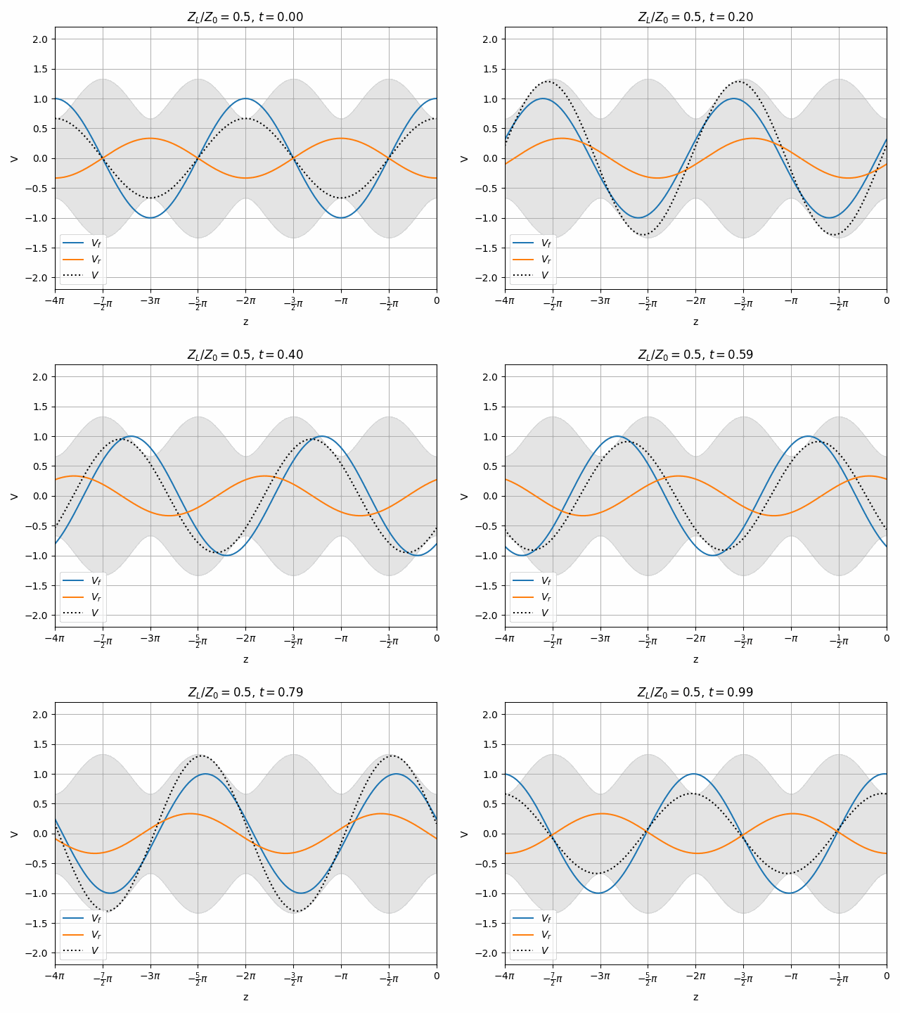
An imperfectly matched but lossy (R \ne 0) load results in a reduced amplitude reflected wave
Standing Wave Ratio
You should notice that not all locations along the transmission line see the same peak voltages (shaded region in the above plots). This is a useful property for determining how well matched a device is. A peak detector can be physically moved along a transmission line to find the peaks and troughs of this standing wave. This ratio is called the Voltage Standing Wave Ratio (VSWR). In practice, VSWR is generally calculated from other measurements.
Peaks in the standing wave will occur wherever the peaks of V_f and V_r align. Similarly, the minimum voltage occurs wherever one wave is at its positive peak and the other is at the negative peak.
\begin{align}
V_{max} &= \left|\hat{V}_f\right| + \left|\hat{V}_r\right| \\
V_{min} &= \left|\hat{V}_f\right| - \left|\hat{V}_r\right|
\end{align}
VSWR is defined as the ratio of these values
\begin{align}
\text{VSWR} &= \frac{\left|\hat{V}_f\right| + \left|\hat{V}_r\right|}{\left|\hat{V}_f\right| - \left|\hat{V}_r\right|} \\
\left|\hat{V}_r\right| &= \left|\hat{V}_f\right| \left|\Gamma\right| \\
\text{VSWR} &= \frac{1 + |\Gamma|}{1 - |\Gamma|}
\end{align}
VSWR is often reported as N:1. I'm not sure why since this carries no additional information than just N but its a convention.
For passive networks (no power is added), 0 < |\Gamma| < 1 so 1 < \text{VSWR} < \infty where 1 is perfectly matched. VSWR does a good job of highlihting poorly-matched networks while making well-matched and decently-matched networks appear similar.
In general, \text{VSWR} < 2 can be considered well matched.
I have mostly seen VSWR used for antennas and system interface specifications. It is particularly useful for bounding worst case mismatch when creating a system cascade but we'll get to that later.
Return Loss
Another way to look at reflections is with return loss. This is really just a decibel way to look at reflected power. Remember that \Gamma is a voltage ratio, not power ratio so return loss is:
\begin{align}
\text{Return Loss} = 20 \log_{10}(|\Gamma|)
\end{align}
It is not uncommon to see this expressed as either negative (the right way) or positive values. In practice nothing has |\Gamma| > 1 so there really isn't any ambiguity regardless of which sign this is presented with.
Example
TODO: add example plots and such
Impedance Transformation
If we were to cut a transmission line at position z and look into the loaded line from the left end, we can determine the input impedance of the combined transmission line + load circuit.
TODO: derive
Quarter Wave Transformer
Note that if a txline is exactly \ell = \lambda/4 in length, this simplifies quite nicely
\begin{align}
Z &= \frac{Z_0^2}{Z_L}
\end{align}
This property is frequently used in microwave networks for a variety of purposes.
One of the simplest uses is to provide ESD protection to a system by adding a shorted \lambda/4 stub (in parallel) near a connector.
\begin{align}
Z_{stub} &= \frac{Z_0^2}{0} \\
&= \infty
\end{align}
So the short looks like an open and the stub disappears at the design frequency, however at much lower frequencies (\ell << \lambda/4) where we have most ESD concerns the short protects downstream devices from voltage spikes. This method typically works above a few GHz, I'm not sure exactly how low it'll work though \lambda/4 becomes ponderously large and the point becomes moot.
\ell = \lambda/2 has an even simpler result
\begin{align}
Z &= Z_L
\end{align}
The reason we see this repetition after only \lambda/2 rather than a full \lambda is because the wave must travel in both the forward and reverse directions along the txline before we see it again. In other words, the total distance travelled by the wave is 2\ell.
I have not found half-wave lines to be very useful in practice since additional line length will result in narrower-band networks, however it can sometimes be useful to escape a particularly tight section in PCB layout.
Smith Charts
A Smith chart is simply a complex plot of \Gamma with grid lines of constant resistance and reactance.
Sometimes lines of constant conductance and susceptance are added in place of or in addition to resistance/reactance if we want to work in admittance rather than impedance. Since a Smith chart is merely showing \Gamma which is dependent on Z_0, the impedance/admittance lines are often labelled with normalized impedance (Z_L/Z_0).
TODO: make plot
If an impedance Z_S is placed in series with a load, we can fall back on circuit theory. Z = Z_S + Z_1
Lets look at cases where Z_S is purely real or purely imaginary.
- If
Z_S = R_S, thenZ = R_S + R_1 + j X_1
Similarly, if an admittance Y_P is placed in parallel (shunt) with the load, then Y = Y_P + Y_1
Again if Y_P is purely real or imaginary,
| Condition | Smith Chart |
|---|---|
| Series transmission line | counter clockwise (VSWR) |
| Series resistor | right (R) |
| Series capacitor | down (X) |
| Series inductor | up (X) |
| Shunt resistor | left (G) |
| Shunt capacitor | up (B) |
| Shunt inductor | down (B) |
TODO: make plots
